(China (Mainland))

Product Summary
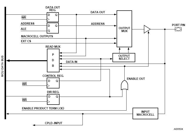
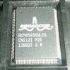
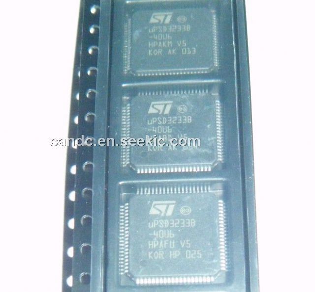
The UPSD32338-40U6 is a Flash Programmable System Device with 8032 Microcontroller Core and 64 Kbit SRAM. The UPSD32338-40U6 has separate 64KB address spaces for Program memory and Data Memory. Program memory is where the 8032 executes instructions from. Data memory is used to hold data variables. Flash memory can be mapped in either program or data space. The UPSD32338-40U6 consists of two flash memory blocks: the main Flash (1 or 2Mbit) and the Secondary Flash (256Kbit). Except during flash memory programming or update, Flash memory can only be read, not written to. A Page Register is used to access memory beyond the 64K bytes address space. Refer to the PSD Module for details on mapping of the Flash memory.
Parametrics
UPSD32338-40U6 absolute maximum ratings: (1)TSTG Storage Temperature: -65 to 125℃; (2)TLEAD Lead Temperature during Soldering (20 seconds max.)(1) : 235℃; (3)VIO Input and Output Voltage (Q = VOH or Hi-Z): -0.5 to 6.5V; (4)VCC Supply Voltage: -0.5 to 6.5V; (5)VPP Device Programmer Supply Voltage: -0.5 to 14.0V; (6)VESD Electrostatic Discharge Voltage (Human Body Model)(2): -2000 to 2000 V.
Features
UPSD32338-40U6 features: (1)fast 8-bit 8032 MCU; (2)dual flash memories with memory management; (3)clock, reset, and supply management; (4)programmable logic, general purpose; (5)communication interfaces; (6)jtag in-system programming; (7)A/D converter four channels, 8-bit resolution, 10μs; (8)timers and interrupts; (9)Single Supply Voltage: 4.5 to 5.5V; -3.0 to 3.6V.
Diagrams