(China (Mainland))

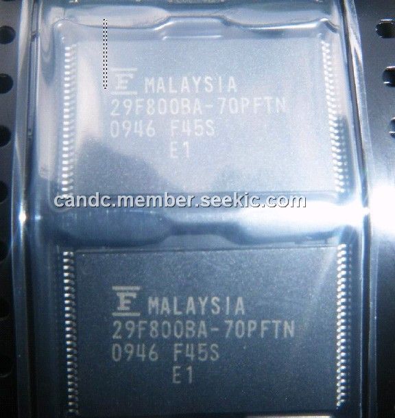
Product Summary
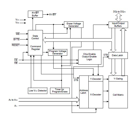
The 29F800BA-70PFTN is an 8M-bit, 5.0 V-only Flash memory organized as 1M bytes of 8 bits each or 512K words of 16 bits each. The MBM29F800TA/BA is offered in a 48-pin TSOP(I) and 44-pin SOP packages. The 29F800BA-70PFTN is designed to be programmed in-system with the standard system 5.0 V VCC supply. 12.0 V VPP is not required for write or erase operations. The 29F800BA-70PFTN can also be reprogrammed in standard EPROM programmers. The standard 29F800BA-70PFTN offers access times 55 ns and 90 ns, allowing operation of high-speed microprocessors without wait states. To eliminate bus contention the device has separate chip enable (CE), write enable (WE), and output enable (OE) controls. The 29F800BA-70PFTN is pin and command set compatible with JEDEC standard E2PROMs. Commands are written to the command register using standard microprocessor write timings. Register contents serve as input to an internal state-machine which controls the erase and programming circuitry. Write cycles also internally latch addresses and data needed for the programming and erase operations. Reading data out of the devices is similar to reading from12.0 V Flash or EPROM devices.
Parametrics
29F800BA-70PFTN absolute maximum ratings: (1)Storage Temperature: -55℃ to +125℃; (2)Ambient Temperature with Power Applied: -40℃ to +85℃; (3)Voltage with respect to Ground All pins except A9, OE, and RESET: -2.0 V to +7.0 V; (4)VCC: -2.0 V to +7.0 V; (5)A9, OE, and RESET: -2.0 V to +13.5 V; (6)ILI Input Leakage Current VIN = VSS to VCC, VCC = VCC Max.: -1.0 to +1.0 μA; (7)ILO Output Leakage Current VOUT = VSS to VCC, VCC = VCC Max.: -1.0 to +1.0 μA.
Features
29F800BA-70PFTN features: (1)Single 5.0 V read, write, and erase Minimizes system level power requirements; (2)Compatible with JEDEC-standard commands Uses same software commands as E2PROMs; (3)Compatible with JEDEC-standard world-wide pinouts; (4)Minimum 100,000 write/erase cycles; (5)High performance 55 ns maximum access time; (6)Sector erase architecture; (7)Boot Code Sector Architecture; (8)Embedded Erase Algorithms; (9)Embedded ProgramTM Algorithms; (10)Data Polling and Toggle Bit feature for detection of program or erase cycle completion; (11)Ready/Busy output (RY/BY)Hardware method for detection of program or erase cycle completion; (12)Low Vcc write inhibit 3.2 V; (13)Erase Suspend/Resume Suspends the erase operation to allow a read data in another sector within the same device; (14)Hardware RESET pin Resets internal state machine to the read mode; (15)Sector protection Hardware method disables any combination of sectors from write or erase operations; (16)Temporary sector unprotection Temporary sector unprotection via the RESET pin.
Diagrams